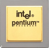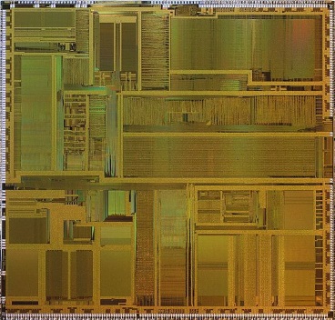
The Pentium P5 processor was introduced in 1993. It used a 5 Volt power supply and had 3.1 million transistors. Fabricated in 0.8-micron bipolar complementary metal oxide semiconductor (BiCMOS) technology, its die measured 16.7 mm by 17.6 mm. It had a 2x8 kb L1 cache, and operated at 50, 60 and 66 MHz.
Innovations Introduced in the P5
• Superscalar Architecture
The Pentium P5 was the first superscalar processor. It has two integer (U and V) pipelines that allow it to complete two instructions per clock cycle. The pipelines had five stages and were served by two 32-byte prefetch buffers.
P5 pipelined floating-point unit had 8 stages. A bug that was discovered in its floating point unit soon after it was released. It was a minor bug, but was blown way out of proportion because Intel didn't recognize and correct it immediately.
• Dynamic Branch Prediction
The Pentium’s branch prediction use a Branch Target Buffer (BTB) to speed up program execution by anticipating branches and ensuring that branched-to code was available in cache.
• 64-bit External Data Bus
A 64-bit external data bus gives the Pentium P5 4GB of memory addressing capability, but, it has only 32-bit internal registers. Internally instructions are broken down into 32-bit instructions and data elements.

pentium die
• On-board Interrupt Controller
The Pentium processor has an on-chip Advanced Programmable Interrupt Controller (APIC). This APIC implementation supports multiprocessor interrupt management, inter-processor interrupt support and multiple I/O subsystem support.
• Parity Checking
Even-parity checking is implemented for the data bus and the internal caches and buffers.
• Separate Code and Data Caches
Separation of code and data caches lessens the fetch and operand read/write conflicts.

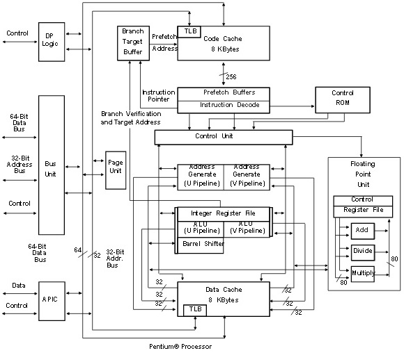
Pentium Schematic
The data cache has two ports, one for each of the two pipes. The data cache has a dedicated Translation Lookaside Buffer (TLB) to translate linear addresses to the physical addresses used by the data cache. The code cache, branch target buffer and prefetch buffers are responsible for getting raw instructions into the execution units of the processor. Instructions are fetched from the code cache or from the external bus. Branch addresses are remembered by the branch target buffer. The code cache TLB translates linear addresses to physical addresses used by the code cache.
• 8 KB Instruction and a Data Cache
Pentium processors include separate code and data caches. Each cache is 8 KB in size. Each cache has a dedicated Translation Lookaside Buffer (TLB) to translate linear addresses to physical addresses.
Pentium P54C
The Pentium P54C was released in 1994 with a 3.3 Volt power supply and was fabricated in 0.6-micron BiCMOS technology. The P54C processor also has a System Management Mode (SMM) for advanced power management for notebooks and other battery-based applications.
More Computer Architecture Articles:
• Using The I2C Bus
• Operating System Memory Page Sharing
• Operating System File Management
• Multilevel Queue CPU Scheduling Algorithm
• Basic Computer Architecture
• Introduction to Microprocessor Programming
• Capacitors in AC Circuits
• Operating System Memory Allocation Methods
• Operating System Process Control Block
• CPU Process Memory Address Binding

