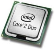
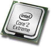
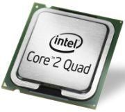
Intel's Core 2 processors, released in July of 2006, are based on the "Core microarchitecture", which Intel calls "Core 2", as apposed to the Pentium's "NetBurst" core, which might be dubbed "Core 1" and was not performance competitive with AMD's Athlon 64 architecture.
The Core 2 architecture is a dual core design, having two cores integrated on a single die. The dual cores use a 65nm manufacturing process to put 291 million transistors on a 143 square mm die. Each core has its own separate 64KB L1 cache that's divided into a 32KB instruction cache and 32KB data cache. The two cores share an L2 cache that can be either 2MB or 4MB.

Core 2 product line features the "Core 2 Duo", and the "Core 2 Extreme". The "Duo" is designed for the high-performance notebook and desktop market, and runs at clock speeds of 1.86 GHz for the E6300 chip, to 2.66 GHz for the E6700 chip. The low-end E6300 and E6400 processors have only 2MB of L2 cache, while the E6600 and E6700 have 4MB of L2 cache

The Core 2 Extreme, designed for the extreme power required by users such as high-end graphics professionals, runs at a clock speed of 2.93 GHz for the X6800 chip.
Core 2 achieves its performance by executing more instructions per clock cycle through a shorter instruction pipeline. Core 2 is also more power efficient, disipating only 65 Watts compared to 130 Watts or more for a high-end Pentium.
- Pipelining is a technique where several instructions, each at a different stage of processing, are in the pipeline being processsed simultaneously, when an instruction reaches the end of the pipeline, its execution is complete.
Core 2 processors have two cores with Intel's Extended Memory 64 Technology (EM64T) and operate with a 1066MHz Front Side Bus (FSB). They feature the Execute Disable Bit (XDB), which prevents viruses from exploiting buffer overrun vulnerabilities. They operate with 0.85 - 1.3625 Volts and use the LGA775 socket.
Core 2 Duo
| Model | Frequency | L2-Cache | FSB MHz | Multiplier |
| E6300 | 1866 MHz | 2048 KiB | 1066 | 7x |
| E6400 | 2133 MHz | 2048 KiB | 1066 | 8x |
| E6600 | 2400 MHz | 4096 KiB | 1066 | 9x |
| E6700 | 2667 MHz | 4096 KiB | 1066 | 10x |
Core 2 Extreme
| Model | Frequency | L2-Cache | FSB MHz | Multiplier |
|---|---|---|---|---|
| X6800 | 2933 MHz | 4096 KiB | 1066 | 11x |
Core 2 Duo Mobile
In August of 2006 Intel released it's "mobile" version of the Core 2 Duo. There's no big change with the mobile version, just lower clock and FSB speeds to reduce the power consumption to 34 Watts so the battery lasts longer. Intel released Socket M for the Core 2 line of mobile processors.
| Model | Frequency | L2-Cache | FSB MHz | Multiplier |
| T5200 | 1600 MHz | 2048 KiB | 533 | 12x |
| T5500 | 1667 MHz | 2048 KiB | 667 | 10x |
| T5600 | 1833 MHz | 2048 KiB | 667 | 11x |
| T7200 | 2000 MHz | 4096 KiB | 667 | 12x |
| T7400 | 2166 MHz | 4096 KiB | 667 | 13x |
| T7600 | 2333 MHz | 4096 KiB | 667 | 14x |
Core 2 Quad

In January 2007 Intel released it's "Quad" processors. Outside of having two dual core Core 2 processors in one package, there's no big change with the Quad Core version. For example, the QX6700 Quad Core is actually two E6700 chips in one LGA 775 package connected together by a 1066 FSB MHz Front side bus.
| Model | Frequency | L2-Cache | FSB MHz | Multiplier |
| Q6600 | 2400 MHz | 2 × 4096 KiB | 1066 | 9x |
| QX6700 | 2667 MHz | 2 × 4096 KiB | 1066 | 10x |
More Computer Architecture Articles:
• Intel's Core i7 Processors
• The Microcontroller Interrupt System
• Operating System Memory Page Sharing
• Multi-Processor Scheduling
• Interrupt Request Lines (IRQs)
• Arduino Microcontroller Development Platform
• Intel's Sandy Bridge Micro-Architecture
• Microcontroller Architectures
• The Android Operating System
• Priority CPU Scheduling Algorithm

